
Thin Film Deposition and Characterization Techniques
Abstract
Thin films are everywhere in the modern world, with many of the technologies we depend upon in daily life being, in turn, dependent upon thin film technology. Chemical bath deposition includes principles of chemical bath deposition (CBD) and concept of solubility product, nucleation and film growth, thin film deposition mechanism in chemical bath deposition. The non-metallic ion source (anions) and metal ion source (cations) then react to form the compound.
The nucleation process plays an important role in determining the crystallinity and microstructure of the resultant film.
From the discussion of deposition techniques which are physical and chemical deposition methods. Physical deposition techniques contains sputtering deposition, electron beam evaporation and physical vapour deposition (PVD) process have been known for over 100 years and also fabrication films on the substrate, as well as the increasement of the pressure in the chamber due to operation of the sources indicates directly that gases or vapors are desorbed. Chemical deposition process is economically effective and has been industrially exploited to large scale. It can be summarized that thin film characterization techniques include X-ray diffraction (XRD), UV-Vis spectrophotometer, scanning electron microscopy, energy dispersive x-ray diffraction, transmission electron microscopy (TEM). X-rays diffraction (XRD) is a rapid and a powerful technique used to study the phase of a crystalline material, information on unit cell lattice parameters, crystal structure, crystal orientation and crystalline size.
Article Information
- Received
- Accepted
- Published
Copyright © 2022 Temesgen Geremew
 This is an open-access article distributed under the terms of the Creative Commons Attribution License, which permits unrestricted use, distribution, and reproduction in any medium, provided the original author and source are credited.
Corresponding author: Temesgen Geremew, Debark University, Department of physics, Debark, Ethiopia. Orcid ID: , https://orcid.org/0000-0002-5144-9508 —
Competing Interests
The authors have declared that no competing interests exist.
Funding
No specific funding statement was provided by the authors.
Data Availability
The data that supports the findings of this study are available within the article.
Acknowledgements
The authors would like to acknowledge Debark and Addis Ababa University.
Citation:
Introduction
Thin-film deposition processes for solid-state device fabrication are needed in many steps in the fabrication process. It is important that compatible deposition processes are selected that do not interfere with the structures already built into the device. The process integration, which has to consider thermal effects, chemical and metallurgical compatibility as well as functional requirements and limitations, is a major consideration in successful process selection. Frequently, the deposition processes have to offer a high degree of flexibility in meeting the demands for specific device requirements. The process selection has to be based on adjusting deposition parameters such as film thickness, uniformity and composition 1. Thin film deposition is the technology of applying a very thin film of material between a few nanometers to about 100 micrometers, or the thickness of a few atoms onto a "substrate” surface to be coated, or onto a previously deposited coating to form layers. Thin film deposition manufacturing processes are at the heart of today’s semiconductor industry, solar panels, disk drives, and optical devices industries 2.
Thin films are everywhere in the modern world, with many of the technologies we depend upon in daily life being, in turn, dependent upon thin film technology. These may range in dimension from an atomic or molecular monolayer—perhaps only a few angstroms thick—to either mono- or multilayer coatings with a thickness of several microns. Such materials may have a huge range of extremely useful properties; they may be, for example, anti-reflective, impervious to oxygen and/orothergases, optically transparently electrically conductive, catalytic, and self-cleaning. Everyday examples featuring thin film technology include, but are not limited to, mobile phones, touch screens, laptops, and tablets 3, 4. Other important applications of thin films include band pass filters as used in gas analysis 5, mirrors used in astronomy 6, 7, 8, protective (e.g., biomedical, anticorrosive, and antimicrobial) coatings 9, architectural glass coatings (e.g., to reflect heat while transmitting visible light) 10, photovoltaic electricity generation 11, 12, and a great many others.
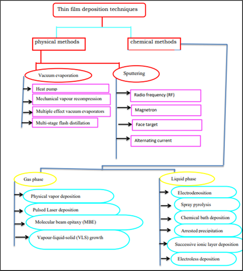
In the present time, thin films can be fabricated in various ways. The techniques can be divided into physical methods (Top-down approach) and chemical (Bottom-up approach) methods as described in Table 113, 14.
Table 1. Classification of thin film deposition techniques
|
The purpose of this review paper is to study deposition techniques of thin film, factor influencing deposition process, thin film characterization and its application. Distinguishing feature between physical deposition technique and chemical deposition technique. In Physical deposition techniques, such as, physical vapor deposition, electron beam’s evaporation and thermal evaporation techniques. In this technique, physical deposition method of the deposition processed through physically can’t take place chemical reaction. However, in chemical deposition techniques contains just like that of chemical vapour deposition, successive ionic layer adsorption and reaction (SILAR) and chemical bath deposition. In chemical deposition techniques which have been used ultrathin film growth. In addition, in chemical deposition method chemical reaction takes place but in physical deposition method doesn’t take place chemical reaction. In case of chemical deposition techniques is to produce high quality films.
Physical Deposition Techniques
Physical Vapor Deposition (PVD)
The main aspects of the physical vapour deposition methods are compiled in Figure 1. Preparation of the films takes place in a vacuum chamber characterized by the residual pressure (in the range of 10-3 – 10-9 Pa) and by the composition and partial vapors ( in high vacuum (HV) range water vapor, oxygen, nitrogen and hydrocarbons, in the ultrahigh vacuum range (UHV) mainly CO, H and He). The vaporized species of the film material components are produced mainly by evaporation or sputter source(s) 15. The characteristics of the emitted species are the flux J, energy E, sizes (atoms, clusters) and ionization state (neutrals or ions) which depend on the material(s) and on the type and working parameters of the source. The kinetic energy, E, of species is 100-200 MeV at thermal evaporation and 5 to 10 eV of sputtered species at floating substrate potential. This last one is in the order of, or larger than the bonding energy in solids. The transport of free species emitted by the sources to the substrate makes possible to manipulate their electrical charge and kinetic energy. However species of the desorbed or residual atmospheric gases/vapours and the products of the possible interactions between the source and the material have to be also considered. An increase of the pressure in the chamber due to operation of the sources indicates directly that gases or vapors are desorbed. This phenomenon has to be considered carefully, because one part of these species impinge directly on the substrate and participate in the structure evolution as unintentional impurities (contaminants).
Figure 1. Main aspects of the physical vapour deposition 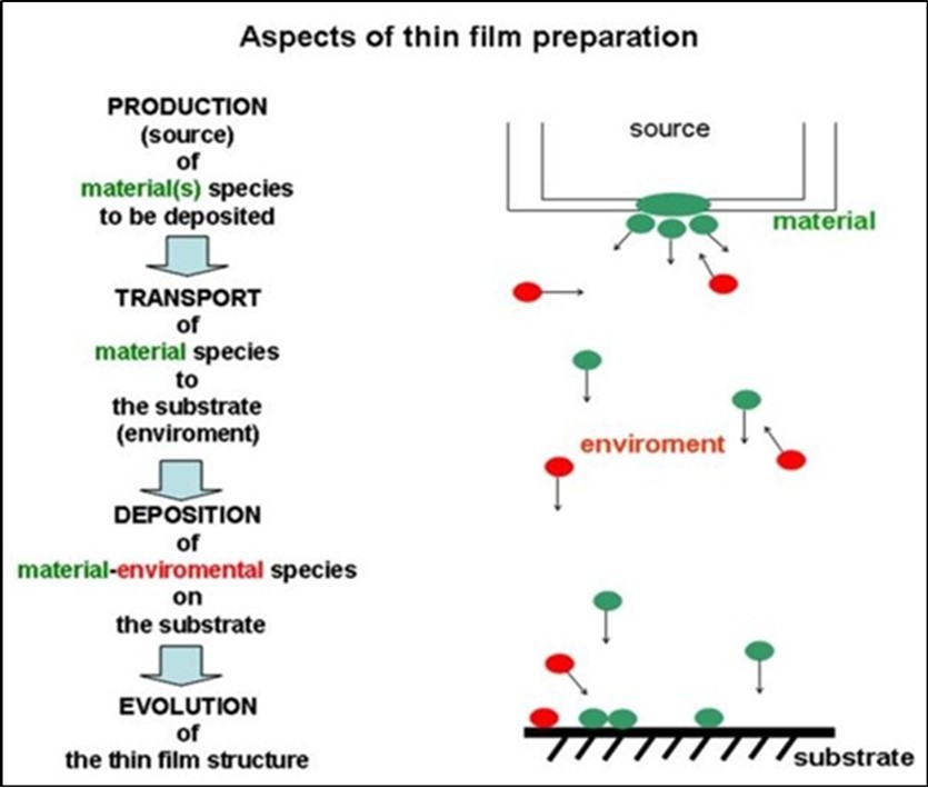
Download figure
By this way the concentration of contaminant species in the condensing vapor beam might be more significant than could be estimated from the total pressure measured in some part of the system 16, 17. Most of these contaminants operate as inhibitors, 18, 19 and might have a remarkable effect both on the structure and properties even at low concentration.
Electron Beam Evaporation
Electron beam evaporation with subsequent vacuum condensation of metals and nonmetals 20, 21. This method is technologically simple, provides rather high coating growth rates (up to several micrometers per minute), and allows a wide range of process parameters 22. In this method the material is bombarded and heated by an electron beam. The electrons are accelerated by 2-6 KV to get high energy. A magnetic field is also applied to focus and bends the electron trajectory.
Thermal Evaporation Technique
One of the oldest techniques used for depositing thin films is thermal evaporation or vacuum evaporation and it is widely used in the laboratory and in industry for depositing metal and metal alloys 23. Thermal evaporation deals with the evaporation of the source materials in a vacuum chamber and condensing the evaporated particles on a substrate. This process is conventionally called vacuum deposition. In this technique, the material can be evaporated either by the heat generated by the resistance of a metal container 24. The possible problems that can be encountered in this technique are the source of material to be vaporized and its purity.
Chemical Deposition Techniques
The chemical deposition process is economically effective and has been industrially exploited to large scale.
Chemical Vapour Deposition (CVD)
Chemical Vapor Deposition (CVD) methods where the films are formed by chemical reaction between incoming species on the substrate. The gas and liquid source are included in this method such as CVD (and varieties plasma-enhanced chemical vapor deposition (PECVD), plasma assisted chemical vapor deposition (PACVD), metal-organo chemical vapor deposition (MOCVD), low pressure chemical vapor deposition (LPCVD)), spray, electrodeposition, chemical Bath, dip coating; sol gel …etc.
Additionally, it requires expensive high temperature reaction furnace and/or vacuum environment, and expensive high vapor pressure compounds. A schematic diagram involving the steps in the process of CVD is illustrated in Figure 2 according to 25.
Figure 2. Schematic representation of CVD processes 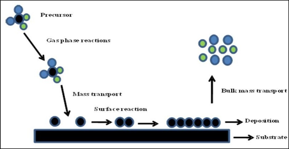
Download figure
In chemical vapor deposition (CVD) the compounds of a vapor phase, often diluted with an inert carrier gas, react at a hot surface to deposit a solid film 26, 27. The importance of CVD is due to the versatility for depositing a large variety of elements and compounds at relatively low temperatures and at atmospheric pressure. Amorphous, polycrystalline, epitaxial, and uniaxially oriented polycrystalline films can be deposited with a high degree of purity. Aspects of CVD include the chemical reactions involved, the thermodynamics and kinetics of the reactors, and the transport of material and energy to and from the reaction site.
The following is a list of examples of some of the common types of chemical reaction used in CVD.
Pyrolysis
The simplest CVD process is pyrolysis, in which a gaseous compound decomposes on a hot surface to deposit a stable residue. Examples are the following: deposition of pyrolytic graphite from methane (CH4), which takes place at a substrate temperature of 22000C; deposition of silicon from monosilane (SiH4), which takes place in the range 800–13500C; and deposition of nickel from carbonyl from Ni(CO)4, which takes place at about 1000C 28.
Reduction
Hydrogen is the most commonly used reducing agent. Examples are deposition of silicon by the hydrogen reduction of silicon tetrachloride, which takes place at about 10000C, and deposition of tungsten by the hydrogen reduction of tungsten hexafluoride, which takes place at about 8000C. Hydrogen reduction is also used to accelerate the pyrolytic process by removal of unwanted byproducts as gaseous hydrogen compounds, for which less energy is required.
Oxidation
Silicon dioxide films can be deposited by the reaction of silane with oxygen.
Nitridation
Silicon nitride films can be deposited by reaction of silane with ammonia.
Carbidization
Titanium carbide films can be deposited by reaction to titanium tetrachloride with methane at a substrate temperature of 18500C.
Chemical-Transport Reaction
For these processes, the transport of the desired material from the source to the substrate on which it is to form a film depends on the difference in equilibrium constants between the reactant source and carrier phase, and the substrate and the carrier phase, when each are held at different temperatures. For example, the deposition of gallium arsenide by the chloride process depends on the reversible reaction

(1)
Where T1 is the temperature of the solid GaAs source, T2 is the temperature of the solid GaAs substrate, and T1 > T2. This allows, in effect, indirect distillation of gallium arsenide from the hot source at temperature T1 to the cooler substrate at temperature T2 through an intermediate gas phase of different chemical composition.
Spray Pyrolysis
In this process the reagents are dissolved in a carrier liquid, which is sprayed onto a hot surface in the form of tiny droplets. On reaching the hot surface the solvent evaporates and the remaining components react, forming the desired material. An example is the formation of cadmium sulfide films by spray pyrolysis of cadmium chloride and thiourea dissolved in water with the substrate at about 3000C 29. Table 2 shows many applications of CVD processes.
Table 2. Application of CVD processes| Thin Film | Application |
| Epi-Si | Semiconductor material |
| a-Si | Solar cells |
| Ge | Tunnel diodes, solar cells |
| SiC | Protective against oxidation |
| BN | Diffusion source, crucible material |
| BP | Photovoltaics |
| AIN | Dielectric, piezoelectric material for acoustic wave beam |
| AIP | Electroluminescent diodes |
| AlAs | Electroluminescent diodes, solar cells |
| AlSb | Solar cells |
| GaN | Electroluminescent diodes |
| GaP | Electroluminescent diodes |
| ZnSe | Photoconductor, laser diodes |
| ZnTe | Electro-optical applications |
| CdS | Photoconductors, laser diodes, solar cells, detectors |
| CdS1-xSex | Lasers |
| Zn1-xCdxS | Lasers |
| Cd1-xHgxTe | Photoconductors, laser, photo diodes |
| Pb1-xSnxTe | Photoconductors, laser, photo diodes |
| Pb1-xSnxSe | Lasers |
| PbS | Photoconductors, lasers |
| PbTe | Infrared detectors |
| PbS1-x Sex | Lasers |
| PbSe | Lasers |
| PbO | Photoconductors |
| SiO2; PSG; BSG; | ASG Passivation, etching mask, gate dielectric in MOS structures |
| Si3N4 | Diffusions masks, oxidation masks, anti-reflection coating in solar cells |
| GaAs | Semiconductor material |
| Gasb | Laser diodes |
| InP | Gun diodes, laser diodes |
| InAs | Laser diodes, Hall effect diodes |
| InSb | Photo electrodes |
| GaAs1-x Px | High temperature rectifiers, electroluminescent diodes, laser diodes |
| InAs1-x Px | Photo cathodes, electro-optical applications |
| InAs1-xSbx | Laser diodes |
| GaAs1-xSbx | Laser diodes, photo cathodes |
| Ga1-xInxAs | Laser diodes, photo cathodes |
| Ga1-xInxP | Luminescent diodes |
| Ga1-xAlxAs | Laser diodes, solar cells |
| InxAl1-xP | Electroluminescent diodes, laser diodes |
| W | Metallization, conductive path in integrated circuits |
| Mo | Schottky diodes, conductive path |
| Ta | Conductive path |
Physicochemical Bases
At the CVD process gaseous chemical compounds, often diluted with an inert carrier gas, react on hot surfaces in the reactor to form solid films, Figure 3. The CVD process can be subdivided as follows:
Figure 3. with the chemical the vapor deposition, e.g., of metals, a precursor molecule at a temperature T1 reacts with hydrogen (H2) to a complex, which deposits itself to the coated surface. At the substantially higher temperature T2 of the substrate the complex decomposes into an organic remainder of R and a metal atom, which forms the nucleus for layer growth with others
Download figure
Production of a reaction gas mixture, Transportation phase, Deposition and film formation.
The relatively high gas pressure is characteristic in the transportation phase. It can amount to between 10mbar and 10bar. The mean free path 𝜆 is small in relation to the dimensions of the recipient and/or the distance source – substrate d. CVD processes occur at small Knudsen numbers Kn

(2)
The high process pressure distinguishes CVD from PVD. Because of the collisions in the gaseous phase of the CVD process, the molecules, which create the film structure, must be sluggish in reaction, so that no powder developed in the gaseous phase and no damaging secondary reactions take place. This means that as original substances not atoms, like in the PVD process, but molecules that are sluggish in reaction must be used. An ideal characteristic curve for a thermal CVD process is shown in Figure 3.
At low temperatures (range I) the deposition process is determined by the reactions taking place at the surface. The deposition is described by Arrhenius law:
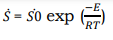
(3)
Where the E the activation energy and R the universal gas constant. At higher temperatures the reaction rates at the surface become so fast that the deposition is
Figure 3 with the chemical the vapor deposition, e.g., of metals, a precursor molecule at a temperature T1 reacts with hydrogen (H2) to a complex, which deposits itself to the coated surface. At the substantially higher temperature T2 of the substrate the complex decomposes into an organic remainder of R and a metal atom, which forms the nucleus for layer growth with others
Figure 4. Ideal CVD characteristics curve, I the deposition process is determined by the reactions taking place at the surface, II determined by the flow in the reactor and approximated temperature- independently, III homogeneous reactions in the gaseous phase
Figure 4. Ideal CVD characteristics curve, I the deposition process is determined by the reactions taking place at the surface, II determined by the flow in the reactor and approximated temperature- independently, III homogeneous reactions in the gaseous phase
Download figure
Figure 5. Different types of CVD characteristics curves, (1) suitable for batch reactor, (3) for high deposition rates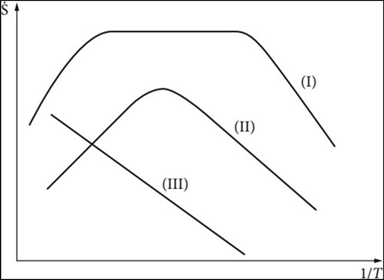
Download figure
Determined by the transport through the gaseous phase. In this range the deposition rate and the uniformity of the film is determined by the flow in the reactor and approximated temperature independently (range II). At still higher temperatures (range III) the deposition is controlled by homogeneous reactions in the gaseous phase, which can finally lead to powder formation. The deposition rate is thereby reduced. Figure 5 shows the different types of characteristic curves. The selection of the operating point on the CVD characteristic curve depends on:
1. The form of the work pieces
2. The film structure.
Figure 5 Different types of CVD characteristics curves, (1) suitable for batch reactor, (3) for high deposition rates
If complicated forms or porous work pieces are to be coated on the inside, then the operating point is always selected within the kinetically controlled range, because of the low deposition rate at which no eluviation of the gaseous phase occurs. With simple forms, e.g., coating of plane surfaces, other aspects are of importance. Thus, for example, the desired film structure requires a defined operating point. This is valid, for example, in the case of the Si epitaxy 30, 31. At the silicon surface silane decomposes according to the chemical equation

(4)
Moreover, the silicon growth rate is proportional to the partial pressure of silane. For cases where the reaction is surface controlled, epitaxial growth proceeds according to the following steps: Mass transfer of the reactant molecules (SiH4) by diffusion from the turbulent film across the boundary film to the silicon surface.
1. Adsorption of the reactant atoms on the surface.
2. The reaction of a series of reactions that occur on the surface.
3. Desorption of the byproduct molecules.
4. Mass transfer of the byproduct molecules by diffusion through the boundary film to the main gas stream.
5. Lattice arrangement of the adsorbed silicon atoms.
The overall deposition rate is determined by the slowest process in the list above. Under steady- state conditions all steps occur at the same rate and the epitaxial film grows uniformly. Depending upon deposition conditions different reactor types is used. For the kinetically controlled range (range I) batch reactors are suitable. The flux plays a subordinated role in this case only. Due to low eluviation’s larger numbers of work pieces can be coated at the same time. In the range II the deposition is strongly affected by the flux, however higher coating rates are to be expected.
Successive Ionic Layer Adsorption and Reaction (SILAR)
SILAR is aqueous solution technique based on sequential reactions at the substrate solution interface for the deposition of thin films. The SILAR was developed by Nicolau for the deposition of zinc and cadmium chalcogenides thin films 32. The adsorption is a surface phenomenon between ions and surface of substrate and is possible due to attraction force between ions in the solution and surface of the substrate. These forces may be cohesive forces or Van der Waals forces or chemical attractive forces. Atoms or molecules of substrate surface possess unbalanced or residual force and hold the substrate particles. Rinsing follows each reaction, which enables heterogeneous reaction between the solid phase and the solvated ions in the solution 33. In spite of its simplicity, SILAR has a number of advantages. It is relatively inexpensive, simple and convenient for large area deposition.
In principle, it is possible to deposit metal chalcogenide thin films using this method on to variety of substrates 34. The starting materials are commonly available and cheap. As it is a chemical method, a large number of varieties of substrates can be coated. Thus, any insoluble surface to which the solution has free access will be a suitable substrate for the deposition.
Figure 6 represents the deposition of thin film using SILAR method. It consists of four different steps such as adsorption, rinsing (a and b), reaction and rinsing (c and d) 33.
Figure 6. Schematic representation of SILAR method (a) cationic precursor and (c) anionic precursor and (b, d) deionised water 35.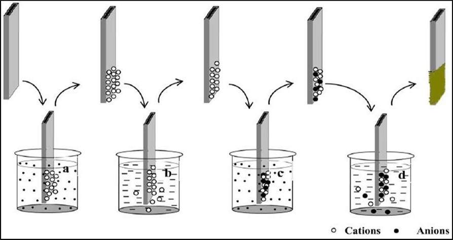
Download figure
Chemical Bath Deposition
Chemical bath deposition (CBD) method is most commonly used because it is a very simple, cost effective and economically reproducible technique that can be applied in large area deposition at low temperature. Chemical bath deposition is used to deposit thin films of a wide-range of materials 36. The deposition mechanism is largely the same for all such materials. A soluble salt of the required metal is dissolved in an aqueous solution, to release cations. The non-metallic element is provided by a suitable source compound, which decomposes in the presence of hydroxide ions, releasing the anions. The anions and cations then react to form the compound 37. In addition, the experimental set up of CBD techniques described in Figure 7 below.
Figure 7. Experimental set up of CBD technique 38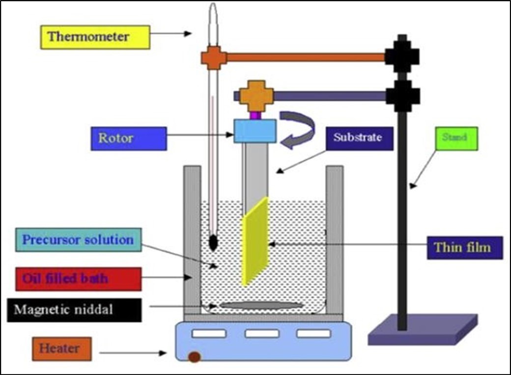
Download figure
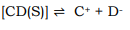
Principles of Chemical Bath Deposition (CBD) and Concept of Solubility Product CBD method is most commonly used because it is a very simple, cost effective and economically reproducible technique that can be applied in large area deposition at low temperature. Chemical bath deposition is used to deposit thin films of a wide-range of materials. The deposition mechanism is largely the same for all such materials. A soluble salt of the required metal is dissolved in an aqueous solution to release cations. The non-metallic element is provided by a suitable source compound which decomposes in the presence of hydroxide ions, releasing the anions. The anions and cations then react to form the compound. This technique is based on the controlled release of metal ion (M 2+) and sulphide (S 2−) or selenide (Se 2−) ions in an aqueous bath in which the substrates are immersed. In this process, release of metal ion (M 2+) is controlled by using a suitable complexing agent 39. The solubility product gives the solubility of a sparingly soluble ionic salt (this includes salts normally termed insoluble). Sparingly soluble salt CD, when placed in water, a saturated solution containing C + and D− ions in contact with undissolved solid CD is obtained and equilibrium established between the solid phase and in the solution as
(5)
Applying law of mass action

(6)
Where K solubility [C+],[D-] and [CD] are concentrations of C+, D- in the solution, respectively. The concentration of pure solid is a constant number i.e.
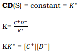
(7) (8) (9)
Since K and K* are constants of KK*is also constant, say Ks,therefore Eq.

(10)
The constant KS is called solubility product (SP) and [C+][D−] is called ionic product (IP). When the solution is saturated the ionic product is equal to the solubility product. When the ionic product exceeds the solubility product (IP/SP = S>1), the solution is supersaturated (where S is degree of super saturation), precipitation occurs and ions combine on the substrate and in the solution to form nuclei [40].
Nucleation and Film Growth
Growth of thin films, as all phase transformation, involves the process of nucleation and growth on the substrate or growth surface. The nucleation process plays an important role in determining the crystallinity and microstructure of the resultant film. For the deposition of thin films with thickness in the nanometer region, the initial nucleation process is even more important. The size and shape of the initial nuclei are assumed to be solely dependent on the change of Gibbs free energy, due to supersaturation, and on the combined effect of surface and interface energies governed by Young's equations 41.
Thin Film Deposition Mechanism in Chemical Bath Deposition
There are four main mechanisms leading to compound formation, whose operation depends on the specific process and reaction parameters. The thin film growth in CBD occurs via the following four possible mechanisms.
1. Simple Ion-by-Ion Mechanism
2. Simple Cluster (Hydroxide) Mechanism
3. Complex-Decomposition Ion-by-Ion Mechanism
4. Complex-Decomposition Cluster Mechanism
Simple Ion-by-Ion Mechanism
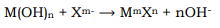
In most of the CBD’s, the ion-by-ion conceptually simplest mechanism, often assumed to be the operative one in general. It occurs by sequential ionic reactions. The general reaction for the mechanism

(11)
The formation of solid MmXn is based on the principle that when the ion product, (Mn+)(Xm−), exceeds the solubility product, Ksp, of MmXn, then MmXn can form as a solid phase, although a larger ionic product may be required if super saturation occurs. If the ion product does not exceed Ksp, no solid phase will form, except possibly transiently due to local fluctuations in the solution, and the small solid nuclei will redissolve before growing to a stable size. For that reason, the precipitation process is an equilibrium rather than as a one-way reaction.
Simple Cluster (Hydroxide) Mechanism
In most of the CBD’s, the preparative conditions are chosen so that the formation of metal hydroxide should be avoided. However, in reality, CBD’s are quite often carried out under conditions where a metal hydroxide (or hydrated oxide) is formed. This might seem to imply that a precipitate of metal hydroxide (M (OH)n) is formed at the start of the CBD. In fact, the metal hydroxide formed is either as a colloid (rather than a precipitate) or as an adsorbed species on the substrate but not in the bulk of the solution. In this case metal chalcogenide (MmXn) is formed by reaction of Xm− ion with the M(OH)n.

(12)
Followed by
(13)
The deposition of the thin film takes place through the condensation of the metal and sulphide/selenide ions on this initial layer which acts as a catalytic surface.
Complex-Decomposition Ion-by-Ion Mechanism
In this mechanism, complex at ion of free metal cations (Mn+) by chalcogenide source (thiourea, thioacetamide) gives M-chalcogenide source complex ion. This is illustrated by the example of CdS deposition from thiourea
(14)
This ion is hydrolyzed by breaking the S-C bond to from CdS.

(15)
This would lead to CdS formation in solution. If Cd2+ is adsorbed on the substrate (either directly or indirectly through a hydroxide linkage) then above reaction occurs and CdS is formed on substrate, the result would be film growth by ion-by-ion. This mechanism is also useful in acidic solution; thioacetamide decomposition at intermediate pH values, particularly in weakly acidic solution (pH ≥ 2) has been suggested to occur through a thioacetamide complex.
Complex-Decomposition Cluster Mechanism
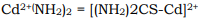
The complex-decomposition cluster mechanism is based on the formation of solid phase, instead of reacting directly with a free anion; it forms an intermediate complex with the anion-forming reagent. For CdS deposited from a thiourea bath the process can be described as:

(16)
Cd(OH)2 is one molecule in the solid phase cluster. This complex or a similar one if contains ammine ligands then decomposes to CdS.

(17)
The S-C bond of the thiourea breaks, leaving the S bond to Cd. It is suggested that Cd(OH)2 forms initially on the substrate and catalyzes the thiourea decomposition. The catalytic effect of the solid surface could be to decompose thiourea to sulphide ion and not necessarily to catalyze the complex- decomposition mechanism 38.
Thin Film Characterization Techniques
The thin-film characteristics are quite different from the respective bulk counterparts. Materials, having at least one of the dimensions in the nanometer scale (less than 100 nm), are known as nanostructured materials, where properties are significantly different because of geometrical restrictions, causing novel physical and chemical properties. Thin films (either it is polycrystalline, or single crystal (epitaxial) or amorphous form) of a thickness (\ 1 lm), possess higher surface energy due to its large surface to volume ratio; thus responsible for different physical, material and chemical properties than their bulk counterpart 42, 43. This scope of tailoring materials’ to create the desired physical properties led to large research activities in many areas such as microelectronics, optoelectronics, and sensors 44. In these devices, precise growth of multiple layers of films (in either amorphous, polycrystalline or epitaxial form) of polymers, metals, semiconductors, and insulators is essential to get the desired outcome. These films are deposited using different techniques such as molecular beam epitaxy (MBE), chemical vapor deposition (CVD), pulsed laser deposition (PLD), sputtering, thermal evaporation, e-beam evaporation, electroplating, and spin coating techniques 42, 45.
Thin film material properties do not always resemble those measured at the bulk level. The application of thin films is becoming increasingly interdisciplinary in nature, leading to new demands for film characterization and properties measurements for both individual films and multilayer films 46.
Measurements and characterization of the film thickness, micro-structure and composition can be carried out using various techniques. They include X-ray diffraction (XRD), UV-Vis spectrophotometer, scanning electron microscopy, energy dispersive x-ray diffraction, transmission electron microscopy (TEM). In this review, we will use for structural analysis X-ray diffraction, for optical analysis UV-Vis spectrometer and for morphological analysis scanning electron microscopy.
X-ray Diffraction (XRD)
X-rays diffraction (XRD) is a rapid and a powerful technique used to study the phase of a crystalline material, information on unit cell lattice parameters, crystal structure, crystal orientation and crystalline size. XRD is widely used to characterize unknown crystalline materials. The working principle of the XRD technique is relied on constructive interference of X-rays and a crystalline sample. In a crystal, the atoms distribute regular in space, which comes into being crystal lattices 47. The structural characterizations have extensively used XRD, which is a non-destructive technique. This technique can be used to determine the crystal structure of metals and alloys, minerals, inorganic compounds, polymers and organic materials. A typical XRD pattern consists of a series of peaks, in which peak intensity is plotted on the Y-axis and diffraction angle (2θ) along X- axis. These peaks are called reflections. The positions of the peaks in XRD pattern depend on the crystal structure of the material while intensities depend on many factors like atomic structure factors, incident intensity, slit width, number of grains etc. 48. X-rays are a type of electromagnetic radiation with a wavelength between 0.1 and 100 Ȧ exhibiting a high energy. In 1895 Wilhelm Conrad Röntgen first discovered X-rays and was therefore awarded the Nobel Prize in Physics in 1901. Hence, it is one of the most fundamental analytical techniques in research fields like solid state chemistry and material science. In a common XRD setup, X-rays are generated in a high vacuum tube 49. Bragg’s law expressed mathematically the crystal diffraction by consider a crystal made of parallel crystals of ions, spaced a distance d apart, and the constructive interference of the rays. By considering a crystal as made out of parallel crystals of ions, spaced a distance d apart Figure 8.
Figure 8. X-ray diffraction from crystal.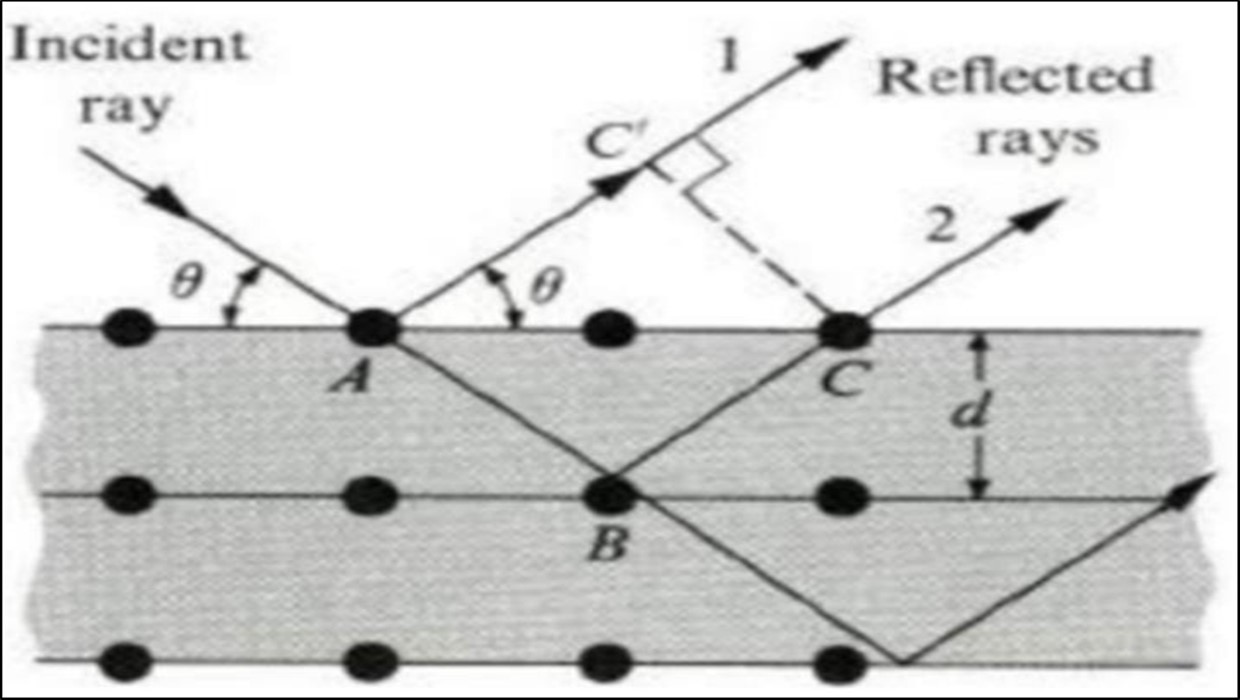
Download figure
The conditions for a sharp peak in the intensity of the scattered radiation are:
1. That the X-rays should be secularly reflected by the ions in any one plane.
2. The reflected rays from successive planes should interfere constructively. Path difference between consecutive rays reflected from adjoining crystal is rays is an integral multiple of the wavelength, That is

(18)
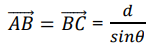
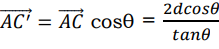
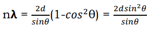
Where ∆d is the path difference and n = 1, 2, 3.
For the rays to interfere constructively, this path difference must be an integral number of wavelength λ. The path difference ∆d between rays 1 and 2 in the Figure 8 is:
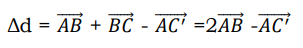
(19)
If and only if this path difference is equal to any integer value of the wave length

(20)
In equating 𝐴𝐵 and 𝐵𝐶, we have assumed that the angles of incidence equal the angles of reflection. When the inter planar distance is denoted by d, it follows from the Figure 8 that
(21)
And

(22)
From which it follow that
(23)

(24)
Putting everything together we get
(25)

Applying the trigonometric relation we get
(26)
Which simplify to arrive at the following condition for constructive interference:

(27)
Where n is the order of diffraction, λ the wavelength of the X-rays, d the distance of the lattice planes and θ is the Bragg angle and the glancing angle between the incident beam and the reflecting crystals. Equation. (27) is known as Bragg’s Law. The possible 2θ values where we can have reflections are determined by the unit cell dimensions.
However, the intensities of the reflections are determined by the distribution of the electrons in the unit cell. The highest electron density is found around atoms 50. XRD measurement allows the calculation of the distance of the lattice planes (d) in the crystal. The grain size of the crystallite is obtained by substituting values of Full Wave Half Maxi-mum (FWHM) in the well-known Debye- Scherrer formula is given by:
 (28)
(28)
where D is grain size of the crystallite, K= 0.94, (λ=1.54059Ǻ ) is the wavelength of the Xray source used, β is the broadening of the diffraction line measured at half of its maximum intensity in radians (FWHM) and θ is the angle of diffraction at the peak 51.
Scanning Electron Microscope (SEM)
The scanning electron microscope (SEM) is one of the most promising technique for generating particle distribution profiles as well as surface characteristics with the possibility to visually reevaluate the data by re-assessing the particle. The technique holds promise for characterization of the size and shape of unknown products with relatively wide distribution profiles from the nanometer to the micron range 52. Also very frequently, scanning electron microscopes are equipped with energy-dispersive X-ray (EDX) detectors, which are used for analyzing local elemental compositions in thin films. However, the possibilities of analysis in SEM go far beyond imaging and compositional analysis. It will be shown that imaging is divided into that making use of secondary electrons (SE) and of backscattered electrons (BSEs), resulting in different contrasts in the images and thus providing information on compositions, microstructures, and surface potentials. Also, it will be demonstrated how important it is to combine various techniques on identical sample positions, in order to enhance the interpretation of the results obtained from applying individual SEM techniques 53.
SEM is one of the most important instruments used for morphology analysis. The SEM generates images by scanning the samples using a focused electron beam. The SEM utilizes a focused electron beam to scan across the surface of the samples then it systematically produces large numbers of signals and these electron signals are converted to a visual signal, which can be displayed on a screen 48.
The types of signals produced by an SEM include secondary electrons; back scattered electrons (BSE), characteristic x-rays, light (cathodoluminescence), specimen current and transmitted electrons. These types of signal all require specialized detectors for their detection that are not usually all present on a single machine. When the beam of electrons strikes the surface of the specimen interacts with the atoms of the sample, signals in the form of secondary electrons, back scattered electrons and characteristics X-rays are generated that contain information about the samples, surface topography, composition, etc. The SEM can produce very high resolution images of the sample surface,revealing details about 1-5 nm in size in its primary detection made i.e. Secondary electron imaging. Characteristics of X-rays are the second most common imaging mode for an SEM. These characteristic X-rays are used to identify the elemental composition of the sample by a technique known as energy dispersive X-ray (EDX). Back-scattered electrons (BSE) that come from the sample may also be used to form an imaging. Back-scattered electron images are often used in analytical SEM along with the spectra made from the characteristics X-rays as clubs to the elemental composition of the sample 54. The schematic image of SEM illustrated as:
UV/VIS Spectrophotometer (UV-VIS)
Ultraviolet-visible spectroscopy (UV-VIS) is a spectroscopy (absorption or reflectance) in the ultraviolet-visible region. The UV-VIS absorption spectroscopy provides information of light absorption as a function of wavelength, which describes the electronic transitions occurring in the measured samples. The UV-VIS spectrophotometer detects the light intensity passing through a sample and compares the detected intensity to incident light intensity (light before passes through the sample). The absorbance A is simple expressed as Beer’s law:

(29)
Where the ratio is I/I0 called transmittance, I is the intensity of light passing through the sample and I0 is the intensity of light before passing through the sample 55. The optical band gap of materials is a very important parameter that determines the application of the films. It is evaluated using the stern relation formula:
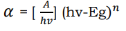
(30)
Where α is absorption coefficient, A is the parameter which depends on the transition probability, ν the frequency of the incident beam, h is Planck’s constant and hv is the incident photon energy. For n =1/2, 2, 2/3, 3 allowed direct, allowed indirect, forbidden direct and forbidden indirect transitions, respectively. For direct band gap materials, n = 1/2, and n = 2, for indirect band gap materials. The plot of α2 or (αhν)2 versus photon energy, hν (in electron volts) with extrapolation of the straight line portion of the curve to zero absorption coefficient (hν axis) gives the band gap energy for direct band gap materials. The plot of α1/2 or (αhν)1/2 versus photon energy hν (in electron volts) with extrapolation to zero absorption coefficient (hν axis) gives the band gap energy for indirect band gap materials 51. And also the absorption band gap (Eg) has been calculated by using the Tauc relation.

(31)
Where A is proportionality constant, h is the Planck’s constant, ν is the frequency of vibration, hν is the photon energy, α is the absorption coefficient and n is either 2 for direct band transitions or 1/2 for indirect band transitions. The absorption coefficient (α) has been calculated using the relation α = 2.303A/t, where t is thickness of the film and A is optical absorbance of film. The direct band gap energy Eg estimated from a Tauc plot of (αhν)2 versus photon energy hν. The value of photon energy (hν) extrapolated to α = 0 gives an absorption edge which corresponds to a band gap Eg 56.
Energy Dispersive X-ray Spectroscopy (EDX or EDS)
Energy dispersive X-ray analysis is a technique to analyze near the surface elements and estimate their proportion at different position, thus giving an overall mapping of the sample. This technique is used in conjunction with SEM. The electron beam strikes a surface of a conducting sample. The energy of the beam is typically in the range 10-20 Kev. This causes X-rays to be emitted from the material. The energy of the X-rays emitted depends on the material under examination. The X-rays are generated in the region about 2 microns in depth, and thus EDX is not truly a surface science technique 54. Energy dispersive X-ray spectroscopy (EDX) in the electron microscope has become an important tool for elemental analysis or chemical characterization for all types of solid material. The bombardment of a material with high energy electrons will result in the emission of characteristic X-rays, whose wavelengths depend on the nature of the atoms in the specimen. For the emission of the characteristic X-rays, an atom has to be excited. There by an electron from an inner shell will be knocked out. This state is instable and the empty state will be filled up from a more energy-rich electron from an outer shell.
Depending from which shell the more energy-rich electron is coming and in which unoccupied inner shell state it goes, the created X-rays are identified as Kα, Kβ and Lα according from which shell the electron was excited and from which shell the electron fills the empty state. The wavelength of this X-ray can be calculated with the following equation:

(32)
Where h is the Planck constant, c the speed of light and ∆E the energy difference of the states involved 49.
Transmission Electron Microscopy (TEM)
Transmission electron microscopy is a good complementary technique to XRD for evaluating the crystallography of materials, and it is conventionally applied to obtain microstructure of materials using a high electron beam (≥ 2ookeV). TEM uses the electrons transmitted through a specimen illuminated with a focused beam of electrons to form image, which is magnified and directed to appear either on a fluorescent screen or layer of photographic film, or to be detected by a sensor such as a charge-coupled device (CCD camera). The electrons are generated by thermionic or field emission accelerated by an electrical field and focused onto the sample using electrical and magnetic fields. A crystalline material interacts with the electron beam mostly by diffraction rather than absorption, although the intensity of the transmitted beam is still affected by the volume and density of the material through which it passes. The specially prepared sample is a very thin (less than 100 nm) slice of material. The electrons pass through the sample and the diffraction pattern and image are formed at the back focus plane and image plane of the objective lens. If we take the back focus plane as the objective plane of the intermediate lens and projector lens, we will obtain the diffraction pattern on the screen. It is said that the TEM works in diffraction mode. If we take the image plane of the objective lens as the objective plane of the intermediate lens and projector lens, we will form image on screen. It is the image mode. The resolution of the TEM techniques is usually 0.3nm. In the most powerful diffraction contrast TEM instruments, crystal structure can also investigated by high resolution transmission electron microscopy (HRTEM), also known as phase contrast imaging as the images are formed due to difference in phase of electron waves scattered through a thin specimen. In HRTEM images, contrast is not intuitively interpretable as the image is influenced by strong aberrations of the imaging lenses in the microscope. Resolution as high as 0.5 Ǻ has been obtained with HRTEM 57, 58, 59. Figure 9, Figure 10
The microstructure of thin films was investigated by transmission electron microscopy (TEM) using a Philips CM20 microscope. In the transmission electron microscopes monochromatic illumination (electron beam with energy from 100 KeV up to 1 MeV) is used to enhance the resolution of TEM Figure 11 60.The principles of image formation in the TEM are the following (Figure 11): (1) the focused electron beam impinge on the extremely thin (30-60 nm) specimen, (2) the electron beam interacts with the specimen. This interaction results in the scattering of the transmitted electron beam. (3) The objective lens forms a diffraction pattern in the back focal plane with electrons scattered by the sample and combines them to generate an image in the image plane (first intermediate image). Thus, diffraction pattern and image are simultaneously present in TEM. In selected area diffraction mode (SAED), an aperture in the plane of the first intermediate image defines the region for which the diffraction is obtained (Figure 11). Which of them appears in the plane of the second intermediate image and is magnified by the projective lens on the viewing screen depends on the intermediate lens. Switching from real space (image) to reciprocal space (diffraction pattern) is easily achieved by changing the strength of the intermediate lens 61.
When taking image (Figure 11), an objective aperture is inserted in the back focal plane of the objective lens to select one or more beams that contribute to the final image (BF, DF, and HRTEM). Including the direct beam into the objective aperture bright field image is formed (BF), while selecting only scattered beams, dark field image (DF) can be received. Switching from real space (image) to reciprocal space (diffraction pattern) is easily achieved by changing the strength of the intermediate lens 61.
Figure 9. Schematic image of SEM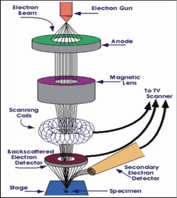
Download figure
Figure 10. Schematic of the relaxation of an inner-shell-excited atom
Download figure
Figure 11. Schematic of a TEM 60, 61.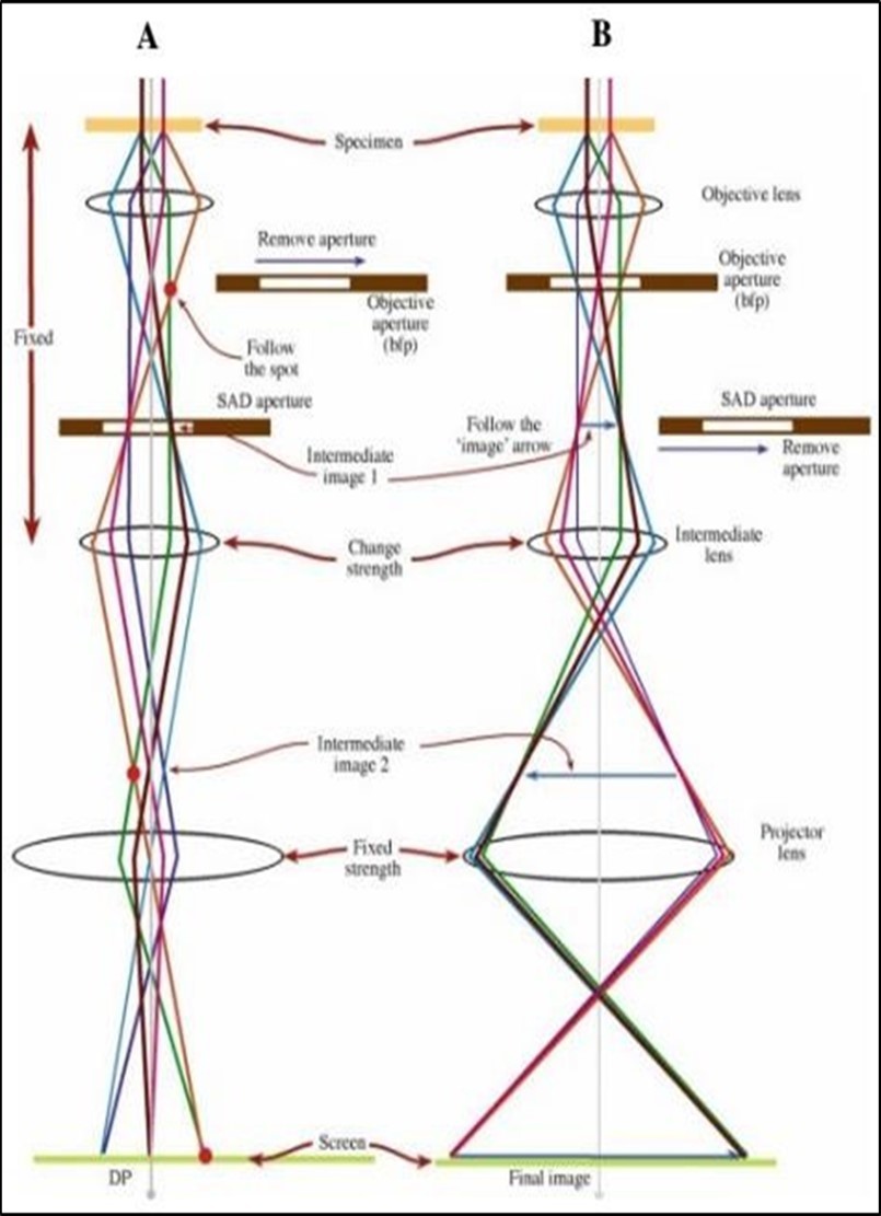
Download figure
Conclusion
In this review, an overview of the deposition methods, thin film characterization and major deposition of thin films has been given. Films may be prepared by many different methods. However, these may usually be classified into chemical or physical methods. In the physical methods the film is deposited from a vapour, maintained at a pressure considerably below that of the atmosphere. Generally, there isn’t an exclusively chemical bath deposition to produce thin films, but there is also chemical vapour deposition, thermal evaporation and electron beam Evaporation to produce thin films. However, in chemical methods the films is deposited from a various chemical reactions to generate a vapour. In this review which is briefly summarized characterization of thin films such as X-ray diffraction, Ultraviolet-visible spectroscopy (UV-VIS), Energy Dispersive X-ray Spectroscopy (EDX or EDS) and Transmission electron microscopy (TEM). The image seen with a transmission electron microscope (TEM) is formed by an electron beam that passes through the specimen. A more recent and extremely useful investigative tool is the scanning electron microscope (SEM). With optical microscopy, the light microscope is used to study the microstructure; optical and illumination systems are its basic elements. X-rays diffraction (XRD) is a powerful nondestructive technique for characterizing crystalline materials.
References
- 2.P R Brown. (2014) Energy level modification in lead sulfide quantum dot thin films through ligand exchange. ACS nano. 8(6), 5863-5872.
- 3.Papadopoulos N, Qiu W, Ameys M, Smout S, Willegems M et al.Touchscreen tags based on thin-film electronics for the Internet of Everything. , Nat. Electron 2019, 606-611.
- 4.Klee M, Beelen D, Keurl W, Kiewitt R, Kumar B et al. (2006) Application of Dielectric, Ferroelectric and Piezoelectric Thin Film Devices in Mobile Communication and Medical Systems. In Proceedings of the 15th IEEE International Symposium on the Applications of Ferroelectrics , Sunset Beach, NC, USA 9-16.
- 5.Fleming L, Gibson D, Song S, Li C, Reid S. (2018) Reducing N2O induced cross-talk in a NDIR CO2 gas sensor for breath analysis using multilayer thin film optical interference coatings. , Surf. Coat. Technol 336, 9-16.
- 6.Birney R, Steinlechner J, Tornasi Z, MacFoy S, Vine D et al. (2018) Amorphous Silicon with Extremely Low Absorption: Beating Thermal Noise in Gravitational Astronomy. , Phys. Rev. Lett 121-191101.
- 7.tefanov S, Vardhan T, Maraka H, Meagher R, Rice P et al. (2020) Thin film metallic glass broad-spectrum mirror coatings for space telescope applications. , J. Non Cryst. Solids X 7, 100050.
- 8.Craig K, Steinlechner J, Murray P, Bell A, Birney R et al. (2019) Mirror Coating Solution for the Cryogenic Einstein Telescope. , Phys. Rev. Lett 122, 231102.
- 9.Robertson S, Gibson D, MacKay W, Reid S, Williams C et al. (2017) Investigation of the antimicrobial properties of modified multilayer diamond-like carbon coatings on 316 stainless steel. , Surf. Coat. Technol 314, 72-78.
- 10.Schaefer C, Bräuer G, Szczyrbowski J. (1997) Low emissivity coatings on architectural glass. , Surf. Coat. Technol 93, 37-45.
- 11.Peumans P, Uchida S, Forrest S. (2010) Efficient bulk heterojunction photovoltaic cells using small-molecular-weight organic thin films. , Mater. Sustain. Energy 94-98.
- 12.Fthenakis V. (2009) Sustainability of photovoltaics: The case for thin-film solar cells. , Renew. Sustain. Energy Rev 13, 2746-2750.
- 14.Y R Toda, K S Chaudhari, A B Jain, D N Gujarathi. (2011) Structural and Optical Properties of CdSe Thine Films Deposted by Chemical bath deposition Technique. Asian. 4(1), 40-43.
- 15.P M Martin. (2010) Deposition technologies: an overview, Handbook of deposition technologies for films and coatings, science, application and technology. 1-31.
- 16.P B Barna. (1983) Impurity effects in the structural development of thin films, in de. Proceedings of the 9th International Vacuum Congress and 5th International congress on solid surfaces, Madrid, Espanole el Vacio , Madrid 382-396.
- 17.P B Barna, Adamik M. (1995) Growth mechanisms of polycrystalline thin films. Science and Technology of Thin Films eds.: Matacotta F. C. and Ottaviani G., World Scientific Publishing Co 1-28.
- 18.Petrov I, P B Barna, Hultman L, J E Greene. (2003) Structural evolution during film growth. , Journal of Vacuum Science and Technology, A 21, 117-128.
- 19.J E Greene. (2010) Thin film nucleation, growth, and microstructural evolution: An Atomic Scale View, in Martin P M, Handbook of deposition technologies for films and coatings, science, Application and Technology, Elsevier. 554-620.
- 20.Harsha K S S. (2006) Principles of Physical Vapor Deposition of Thin Films, Elsevier. , Great Britain 400.
- 21.Laukaitis G, Ju. (2005) Dudonis, D.Milcius, Deposition of YSZ thin films using electron beam evaporation technique. , Mater. Sci 11, 268-271.
- 22.Yu G, A V Tyunkov, D B Zolotukhin, E M Oks. (2016) Electron beam evaporation of boron for ion-plasma coating synthesis at forevacuum pressures. , J. Appl. Phys 120, 233302.
- 23.D M Mattox. (2010) . Handbook of Physical Vapor Deposition (PVD) Processing, 2nd Ed., Elsevier/ William Andrew, ISBN 978-0815520375.
- 25.Akhtar M. the University of Manchester, UK (2013) Synthesis of Iron Chalcogenide Nanocrystals and Deposition of Thin Films from Single Source Precursors. PhD Thesis
- 27.Wahl G, Davies P B, Bunshah R F, Joyce B A, Bain C D et al. (2000) Thin Films” Ullmann’s Encyclopedia of Industrial Chemistry. , Weinheim
- 28.Tavares J, Swanson E J, Coulombe S. (2008) . Plasma Synthesis of Coated Metal Nanoparticles with Surface Properties Tailored for Dispersion. Plasma Processes and Polymers 5(8), 759.
- 29.Chamberlain R R, Skarman J S. (1966) Chemical spray deposition process for inorgqanic films. , J Electrochem Soc 113(1), 88.
- 31.Simmler W. (2005) Silicon Compounds, Inorganic”, Ullmann’s Encyclopedia of Industrial Chemistry. , Weinheim
- 32.Y F Nicolau. (1985) Solution deposition of thin solid compound films by a successive ioniclayer adsorption and reaction process. , Applications of Surface Science 22(23), 1074.
- 33.S D, C D Lokhande. (2000) Deposition of cobalt sulphide thin films by SILAR methods and their characterization. , Indian Journal of pure and Applied Physics 38, 48-52.
- 34.C D Lokhande, H M Pathan. (2004) Deposition of metal chalcogenide thin films by successive ionic layer adsorption and reaction (SILAR) method. , Bulletin of Materials Science 27(2), 85-111.
- 35.Mani P, Manikandan K, A J Ramya, A I seelan, S et al. (2014) . , Influence of Molar Concentrations on Optical Properties of Copper Sulphide Thin Films by SILAR Method. Int.J. ChemTech Res 6(7), 3573-3578.
- 38.Pawar S. (2011) Recent status of chemical bath deposited metal chalcogenide and metal oxide thin films. Current Applied Physics. 11(2), 117-161.
- 39.A O. (2012) Investigating the Optical Properties of Zinc Sulphide Thin Films Deposited from Chemical Acidic Baths.
- 40.Mane R, Lokhande C. (2000) Chemical deposition method for metal chalcogenide thin films. Materials Chemistry and Physics. 65(1), 1-31.
- 41.Tadmor R. (2004) Line energy and the relation between advancing, receding and Young contact angles,Langmuir. 20(18), 7659.
- 44.Muralt P. (2000) Ferroelectric thin films for micro-sensors and actuators: a review. , J. Micromech. Microeng 10, 136-146.
- 45.Sze S M. (2008) Semiconductor Devices: Physics and Technology, 2nd edn. (Wiley India Pvt. , Chichester
- 46.Waters P. University of South Florida (2008) Stress analysis and mechanical characterization of thin films for microelectronics and MEMS applications.
- 47.Chey C O. (2014) Synthesis of ZnO and transition metals doped ZnO nanostructures, their characterization and sensing applications. ping.
- 49.Wochnik A. (2012) Synthesis and characterization of nanostructured copperindiumdisulfide and titaniumdioxide thin films for solar cell application. lmu..
- 51.Nwanya A. (2013) Structural and optical properties of chemical bath deposited silver oxide thin films: role of deposition time. Advances in Materials Science and Engineering .
- 52.Sahoo S, C K, S C Mishra, U N Nanda. (2011) Scanning Electron Microscopy as an analytical tool for particle size distribution and aspect ratio analysis of Ciprofloxacin Mucoadhesive Polymeric suspension. , IJRRAS 6(1), 94-100.
- 53.Abou-Ras D, Kirchartz T, Rau Uwe. (2011) Advanced Characterization Techniques for Thin Film Solar Cells,Wiley-VCH. , Germany
- 54.Joshi M, Bhattacharyya A, S W Ali. (2008) Characterization techniques for nanotechnology applications in textiles.
- 55.Kolmakov A, V.Analyte multi-sensor for the detection and identification of analyte and a method of using the same. 2013, Google Patents.
- 56.Triloki T, Rai R, Singh B. (2013) Absorbance and Transmittance measurement of CsI thin films. , in DAE Symp. Nucl. Phys
- 57.Kisielowski C. (2008) Detection of single atoms and buried defects in three dimensions by aberrtion-corrected electron microscope witth 0.5 Ǻ information limit, microscopy and microanalysis 14:. 469.
- 58.shindo D, kenji H. High Resolution Electron Microscopy for Materials Science (Springer Japan,1998).
- 59.Spence J. (2008) High Resolution Electron Microscopy Monographs on the physics and chemistry of Materials. (OUP Oxford,2008)
Cited by (14)
This article has been cited by 14 scholarly works according to:
Citing Articles:
Emergent Materials (2025) OpenAlex Crossref Semantic Scholar
Surfaces and Interfaces (2025) OpenAlex Semantic Scholar
Transactions of Nonferrous Metals Society of China (2025) OpenAlex Crossref Semantic Scholar
Metals (2025) OpenAlex Crossref Semantic Scholar
Elsevier eBooks (2024) OpenAlex
ACS Omega (2024) OpenAlex Crossref Semantic Scholar
Jurnal Fisika dan Aplikasinya (2023) OpenAlex Semantic Scholar
International Journal for Research in Applied Science and Engineering Technology (2023) OpenAlex
Results in Optics (2023) OpenAlex Crossref
Coatings (2023) OpenAlex Semantic Scholar
Journal of the mechanical behavior of biomedical materials/Journal of mechanical behavior of biomedical materials (2022) OpenAlex
Journal of Chemical Engineering Research Updates (2022) OpenAlex Crossref